25+ Pcb Design Rules Motif Minimalis
Poin pembahasan 25+ Pcb Design Rules Motif Minimalis adalah :
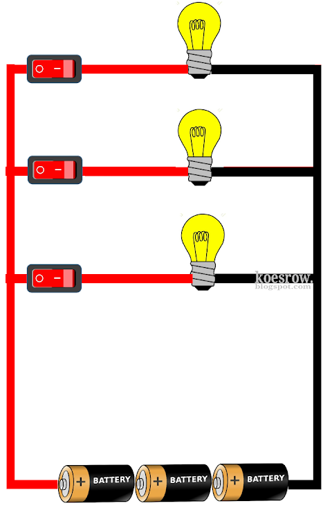
25+ Pcb Design Rules Motif Minimalis. Berikut Penjelasan lengkap tentang fungsi komponen-komponen skema pcb dari yang aktif hingga pasif, prinsip cara kerjanya serta simbol yang wajib difahami. Perhatikan komponen skema pcb jenis resistor berikut yang dilengkapi dengan gambar. Simak ulasan terkait skema pcb dengan artikel 25+ Pcb Design Rules Motif Minimalis berikut ini

Running Design Rules Check in Cadence PCB Editor Sumber : esdresources.blogspot.com

PCB Information Sumber : pcbinfo.blogspot.com

Rigid Flex Circuit Board Gerber Layout Guidelines Webinar Sumber : www.youtube.com

Miniaturization Using Low cost PCB Technology Sumber : www.designworldonline.com

PCB Design Rules Build Electronic Circuits Sumber : www.build-electronic-circuits.com

17 PCB design part IV design rules check YouTube Sumber : www.youtube.com

PCB Prototype Fabrication Manufacturer PCB Prototype in Sumber : www.shenzhen2u.com

PCB Design Rules Build Electronic Circuits Sumber : www.build-electronic-circuits.com
schematic., BOM., mechanical outline., key component locations., mechanical height constraints., current ratings for any power nets., inspection standards - Class 1, 2, or 3?, manufacturing process., 1Adopt DIY approach in making schematic. ..., 2Properly space the components. ..., 3Do not place traces at right angle. ..., 4Ensure same orientation while placing components. ..., 5Use different wiring directions between two consecutive layers. ..., 6Select the line width for facilitating easy current flow. ..., 7Creating ground plane.,

PCB Information Sumber : pcbinfo.blogspot.com

Watch videos FEDEVEL Academy Part 2 Sumber : www.fedevel.com

PCB LAYOUT AUTHORITY Ethernet Component Layout Guidelines Sumber : pcb1001.blogspot.com

PCB Design Guidelines Eurocircuits Sumber : www.eurocircuits.com

PCB Design Rules Reference Online Documentation for Sumber : documentation.circuitstudio.com

Pcb design guidelines Sumber : www.slideshare.net

KiCAD design rules Eurocircuits Sumber : www.eurocircuits.com
schematic., BOM., mechanical outline., key component locations., mechanical height constraints., current ratings for any power nets., inspection standards - Class 1, 2, or 3?, manufacturing process., 1Adopt DIY approach in making schematic. ..., 2Properly space the components. ..., 3Do not place traces at right angle. ..., 4Ensure same orientation while placing components. ..., 5Use different wiring directions between two consecutive layers. ..., 6Select the line width for facilitating easy current flow. ..., 7Creating ground plane.,
25+ Pcb Design Rules Motif Minimalis. Berikut Penjelasan lengkap tentang fungsi komponen-komponen skema pcb dari yang aktif hingga pasif, prinsip cara kerjanya serta simbol yang wajib difahami. Perhatikan komponen skema pcb jenis resistor berikut yang dilengkapi dengan gambar. Simak ulasan terkait skema pcb dengan artikel 25+ Pcb Design Rules Motif Minimalis berikut ini
Running Design Rules Check in Cadence PCB Editor Sumber : esdresources.blogspot.com
Top PCB Design Guidelines for PCB Designers PCB Design
Eurocircuits PCB Design Guidelines have been created to help design engineers create PCB layouts that are Right first Time for Manufacture

PCB Information Sumber : pcbinfo.blogspot.com
Constraining the Design Design Rules Altium Designer
Rigid Flex Circuit Board Gerber Layout Guidelines Webinar Sumber : www.youtube.com
The Engineer s Guide To High Quality PCB Design
The Basic Design Process The ideal PCB design starts with the discovery that a PCB is needed and continues through the final production boards Fig 1 After determining why the PCB is needed
Miniaturization Using Low cost PCB Technology Sumber : www.designworldonline.com
PCB Design Guidelines Eurocircuits Eurocircuits PCB
PCB Design Rules Build Electronic Circuits Sumber : www.build-electronic-circuits.com
PCB Design Layout Guidelines Hints Tips Electronics
17 PCB design part IV design rules check YouTube Sumber : www.youtube.com
PCB Design Rules Build Electronic Circuits
24 09 2020 Here you can either specify the rules by hand which is a little bit cumbersome or you can load a design rule file by clicking the Load button Many manufacturers has a pcb design rules file for Eagle ready to be downloaded so that you only need to load it
PCB Prototype Fabrication Manufacturer PCB Prototype in Sumber : www.shenzhen2u.com
PCB Design Rules Build Electronic Circuits Sumber : www.build-electronic-circuits.com
schematic., BOM., mechanical outline., key component locations., mechanical height constraints., current ratings for any power nets., inspection standards - Class 1, 2, or 3?, manufacturing process., 1Adopt DIY approach in making schematic. ..., 2Properly space the components. ..., 3Do not place traces at right angle. ..., 4Ensure same orientation while placing components. ..., 5Use different wiring directions between two consecutive layers. ..., 6Select the line width for facilitating easy current flow. ..., 7Creating ground plane.,

PCB Information Sumber : pcbinfo.blogspot.com
Watch videos FEDEVEL Academy Part 2 Sumber : www.fedevel.com
PCB LAYOUT AUTHORITY Ethernet Component Layout Guidelines Sumber : pcb1001.blogspot.com
PCB Design Guidelines Eurocircuits Sumber : www.eurocircuits.com
PCB Design Rules Reference Online Documentation for Sumber : documentation.circuitstudio.com
Pcb design guidelines Sumber : www.slideshare.net
KiCAD design rules Eurocircuits Sumber : www.eurocircuits.com


0 Comments